Introduction to band gaps and band structures
In this exercise we study some of the key properties of materials for photovoltaic applications. In the first part of the exercise you will be given a semiconductor material and you are requested to investigate:
atomic structure
band gap
band gap position
band structure
compare how different exchange correlation functionals perform
We will use the ASE and GPAW packages, and at the end of this excercise, you will write your own scripts and submit them to the supercomputer. You will be asked to compare your results to each other and to discuss your results with other groups studying different materials.
Atomic structure
As you have already learnd in the previous session, when investigating the electronic structure of a material, the first thing to do is to find the atomic positions by relaxing the atoms, i.e. minimizing the forces.
Here is some information to help you build the ase.Atoms object:
Silicon crystalizes in the diamond structure with lattice constant \(a=5.43\) Å
Germanium crystalizes in the diamond structure with lattice constant \(a=5.66\) Å
Diamond has diamond structure (!) with lattice constant \(a=3.56\) Å
CdTe crystalizes in the zincblende structure with lattice constant \(a=6.48\) Å
GaAs crystalizes in the zincblende structure with lattice constant \(a=5.65\) Å
Monolayer BN centered in a hexagonal unit cell with \(a=2.5\) Å (and \(7\) Å of vacuum at each side to prevent it from interacting with its periodic copies) and a basis of \((0,0)\) and \((0, a / \sqrt{3})\)
The first thing you should do is to create an ase.Atoms object (click the link to see ways to build atoms objects). In order to do so, you might find it useful to use one of the crystal structures included in ase.build.bulk() (hint: if you have an element of the IV group you might be interested to follow this link ase.build.bulk()) or you might have to create a list/array for the atomic positions and another one for the unit cell and then create an atoms object (hint: see above).
# basic imports
import numpy as np
from ase import Atoms
from ase.build import bulk
Si = ...
Ge = ...
C = ...
CdTe = ...
GaAs = ...
BN = ...

atoms = ...
label = '...'

# view(atoms) # check your initial structure
We are now going to relax the structure. To do so, we need to add a calculator, GPAW, to get DFT energies, and forces. We are going to use PBE exchange correlation functional.
Since we are going to relax the unit cell, we need to use the plane wave mode, since it is the only that includes the stress-tensor. In order to do so, remember this mode requires you to specify the plane wave cut-off (hint: We recommend plane wave cut-off of \(600\) eV and the k-point mesh size could be \((6,6,6)\) if you want it to run reasonably fast and to get a reasonable result). We will discuss convergence further in the next section.
The materials we are looking at are semiconductors. Thus, the default value for the Fermi-Dirac smearing (i.e. occupations function) is too high (it is set up to \(0.1\) eV to work with metals). We recommend setting it to \(0.01\) eV.
These links might be helpful for you:
from gpaw import GPAW, PW, FermiDirac
xc = ...
occupations = FermiDirac(...)
mode = ...
kpts = ...
# We create the calculator object
calc = GPAW(xc=xc,
            txt=label + '_relax.txt',
            occupations=occupations,  # smearing the occupation
            mode=mode,  # plane wave basis
            kpts=kpts)

atoms.calc = calc
We are going to relax the atomic positions and the unit cell at the same time. To do so, we are going to use the ase.filters.UnitCellFilter and the ase.optimize.BFGS (or QuasiNewton) optimizer.
from ase.filters import UnitCellFilter
from ase.optimize import BFGS
filt = ...
op = ...
fmax = ...
# Run the optimization. This will take some time, do not get nervous.
# Only if it takes longer than 4-5 minutes or if it does not print anything
# contact us :)
op.run(fmax=fmax)

# save the results in a file
calc.write(label + '_gs.gpw')
Make sure that you have understood the difference of optimizing a bare atoms object and using a filter!
Bonus: You can attach a trajectory file (filename.traj) to the optimizer and visualize the trajectory using ase gui filename.traj.
Band gap and band structure
We are now going to illustrate how to compute the band gap and obtain the band structure for a toy example with GPAW. You will be writing and submitting meaningful calculations in the next section of this exercise, so do not worry too much about the parameters, we know they are not a good choice and the band structures might look bad.
The starting point for this section (and you might also want to use it in your own scripts) will be the PBE relaxed structure from the previous section:
label = ... # Use the same label as in the previous exercise
from ase.io import read
from gpaw import GPAW, PW, FermiDirac

# Add GPAW's relevant submodules again if you have restarted
# the kernel or if you are copy and pasting to a script

# read only the structure
atoms = read(label + '_gs.gpw')
We are now going to restart the calculator and recompute the ground state, saving it to a new gpw file. As we are dealing with small bulk system, plane wave mode is the most appropriate here. To speed up the computations for this toy example, we use a plane wave cut-off of \(200\) eV and a very coarse k-point mesh \((2,2,2)\). For production-level computations, it is generally a good idea to choose a finer kpoint mesh and higher cut-off for the band structure. Additionally, we are going to use LDA, which is faster than PBE but not very good at predicting bandgaps (yes, we know, you are going to get a silly value here).
# self consistency in LDA
calc = GPAW(mode=PW(200),
            xc='LDA',
            kpts=(2, 2, 2),
            occupations=FermiDirac(0.01))
atoms.calc = calc
Let’s use this calculator to get the energy, the valence band maximum (VBM), the conduction band minimum (CBM), and the band gap, as the difference of the two of the VBM and the CBM.
For the VBM and CBM, we are going to use the `get_homo_lumo()` method of the calculator, see gpaw.calculator.GPAW for more information. This method returns the energy of the highest Kohn-Sham occupied orbital (called HOMO here) and the energy lowest Kohn-Sham unoccupied orbital (the LUMO). We are going to compute the band gap at this level of theory from the difference between both.
# Potential energy
E = ...
vbm = ...
cbm = ...
# Potential energy
E = E
vbm, cbm = vbm, cbm

print('E=', E)
print('VBM=', vbm, 'CBM=', cbm)
print('band gap=', cbm - vbm)
bs = calc.band_structure()
bs.plot(filename=label + '_bandstructure_LDA.png',
        show=True,
        emin=-10,
        emax=10)
# Save the ground state to file
calc.write(label + '_gs_LDA.gpw')
Band structure
Next, we calculate eigenvalues along a high symmetry path in the Brillouin zone. You can find the definition of the high symmetry k-points for the fcc lattice in ase.dft.kpoints.special_points.
If your system is a fcc or the diamond structure, then your path may look something like ‘GXWKL’. For BN, ‘GMKG’.
For the band structure calculation, the density is fixed to the previously calculated ground state density, and as we want to calculate all k-points, symmetry is not used (symmetry=’off’).
# Write the number of bands you are going to compute here, try 2x nbands
nbands = ...
# Write your path here e.g. GXWKL/GMKG
path = ...
# Your number of occupied orbitals comes here, e.g. 8/'occupied'
convergence = ...
# Restart from ground state and fix potential:
calc = GPAW(label + '_gs_LDA.gpw').fixed_density(
    nbands=nbands,
    symmetry='off',
    kpts={'path': path,
          'npoints': 60},
    convergence=convergence)
Finally, we compute the band structure using ASE’s ase.spectrum.band_structure.BandStructure.
bs = calc.band_structure()
bs.plot(filename=label + '_bandstructure_LDA.png',
        show=True,
        emin=-10,
        emax=10)
# You can also save the band structure data in a .json file
bs.write(label + '_bandstructure_LDA.json')
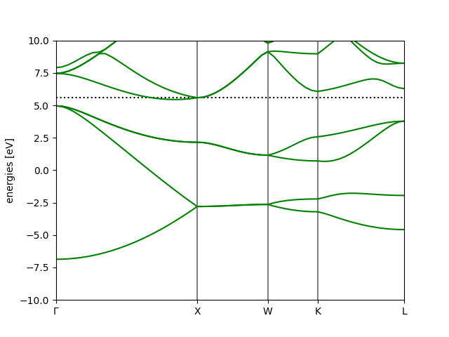
The following image shows the bandstructure we obtain for Silicon.
Convergence (optional but recommended)
In this section, we study the convergence of the results with the parameters that improve the completeness of the basis. Numerical convergence of DFT calculations should always be checked to avoid obtaining spurious results that are caused by a very coarse discretization. In this tutorial you can find an example on how to find a converged lattice constant for aluminum: Finding lattice constants.
Note: If your are running out of time to complete the exercise (i.e., you are left 20 minutes), contact us, we will help you to jump to the next section. You might be able to come back to discuss convergence in DFT in the last day of the summer school.
Look at what happened to the results in the previous section? Did they look reasonable, or did something go wrong? We suggest that you play around with the number of k-points and the plane wave cut-off rerunning the previous band structure example. Increasing their value produces better results, but also increases the computation time.
Finally, we suggest you to explore the convergence of the band gap as in the tutorial for the lattice constant.
The band gap with different exchange correlation functionals
You are now about to complete the last part of the exercise. Now that you know how to do ground state plane wave calculations and to find the band structure of a semiconductor, we ask you to discuss the effect of choosing a functional at a given level of theory. We propose you to study the results with the following functionals:
LDA (the one you have just used)
PBE
RPBE
mBEEF
mBEEF is an meta GGA exchange correlation functional inspired from Bayesian statistics. An essential feature of these functionals is an ensemble of functionals around the optimum one, which allows an estimate of the computational error to be easily calculated in a non-self-consistent fashion. Further description can be found in:
J. J. Mortensen, K. Kaasbjerg, S. L. Frederiksen, J. K. Nørskov, J. P. Sethna, and K. W. Jacobsen (2005). Phys. Rev. Lett. 95, 216401
Wellendorff, J., Lundgaard, K. T., Jacobsen, K. W., & Bligaard, T. (2014). The Journal of Chemical Physics, 140(14), 144107.
To complete this part of the exercise, we suggest that you write scripts and submit them (i.e. write one script for each functional) so that they can run in parallel. As a guide, you can use the LDA calculations you have already done.
Remember to choose a k-point mesh and an plane energy cut-off that make sense. In case of doubt, just ask.
You do not need to relax the structure again, the PBE relaxed structure you have saved to a gpw file in the beginning is good enough. Your script can just read it. :)
Your script should contain a ground state calculation with the functional you are studying. We suggest you print E, VBM, CBM and the gap to a file, together with the functional, so that you can use them for the discussion the last day of the summer school. You should save the ground state to a gpw file (it is a good idea to give different names to the files of different xc functionals) and restart the calculator from that file to compute the band structure. Save the plot to a png file and the data to a .json.